







IBM Breaks the 1 Nanometer Barrier: What the World’s First 0.7nm Chip Means for the Future of AI and Computing
For decades, the semiconductor industry has been driven by a simple goal: pack more transistors into smaller spaces to deliver greater performance and efficiency. However, as transistor dimensions approached atomic scale, many experts questioned how much further chip manufacturers could push traditional silicon technology.
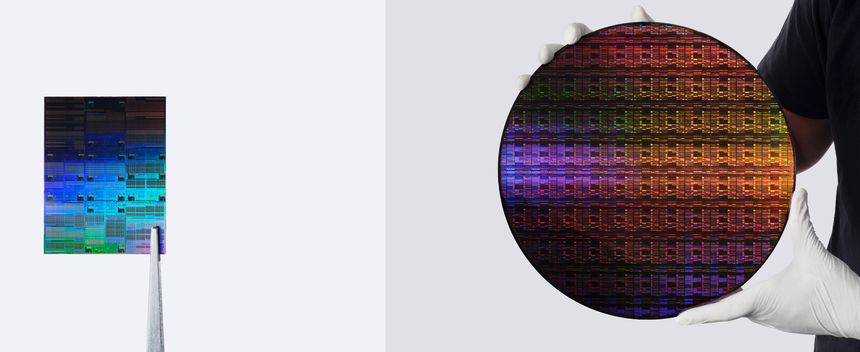
On June 25, 2026, IBM announced a breakthrough that may redefine the future of semiconductors: the world’s first sub–1 nanometer chip technology, built using a new 0.7nm (7 angstrom) process node and an innovative 3D “nanostack” transistor architecture. [newsroom.ibm.com]
Why This Announcement Matters
The semiconductor industry has been approaching the physical limitations of conventional chip scaling for years. As transistors become smaller, engineers face increasingly difficult challenges involving heat, power consumption, electron leakage, and manufacturing complexity. [newsroom.ibm.com]
IBM’s breakthrough demonstrates that continued scaling remains possible even below the 1nm threshold. The company successfully developed a new transistor design that moves beyond traditional planar and nanosheet architectures into a true three-dimensional structure. [newsroom.ibm.com]
The implications extend far beyond faster computers. This technology could accelerate advancements in:
- Artificial Intelligence
- Cloud Computing
- Edge Computing
- Mobile Devices
- Data Centers
- High-Performance Computing
- Future Quantum-Classical Hybrid Systems [newsroom.ibm.com]
Understanding IBM’s Nanostack Architecture
The most significant aspect of the announcement isn’t simply the size of the transistor. It’s the architecture that made the breakthrough possible.
IBM’s new Nanostack design introduces the industry’s first known three-dimensional nanosheet-based transistor architecture. Instead of continuing to shrink transistors on a flat surface, IBM vertically stacks and staggers transistor layers, dramatically increasing transistor density while improving power efficiency. [newsroom.ibm.com]
Key advantages include:
1. Greater Density
The new 0.7nm chip packs nearly 100 billion transistors onto a fingernail-sized chip, almost double the density of IBM’s 2nm chip introduced in 2021. [newsroom.ibm.com]
2. Improved Performance
IBM projects up to 50% more performance compared to its previous 2nm technology. [newsroom.ibm.com]
3. Reduced Power Consumption
The technology can deliver up to 70% greater energy efficiency, potentially reducing power requirements for AI workloads and hyperscale cloud environments. [newsroom.ibm.com]
4. Material Optimization
Nanostack allows different material combinations within each transistor layer, enabling engineers to optimize power and performance independently within the stack. [newsroom.ibm.com]
As AI adoption continues to surge, organizations are struggling with the infrastructure demands required to support modern Large Language Models (LLMs), generative AI platforms, and advanced machine learning workloads.
Today’s AI data centers face three primary challenges:
- Massive power consumption
- Thermal management issues
- Escalating infrastructure costs
The efficiency gains promised by IBM’s 0.7nm technology directly address these concerns. A 70% improvement in energy efficiency could significantly reduce operating costs while enabling larger and more sophisticated AI models. [newsroom.ibm.com]
IBM also reported that its nanostack architecture achieves approximately 40% SRAM scaling, helping support the high-bandwidth memory requirements of next-generation AI systems. Memory throughput and latency have become critical bottlenecks for AI infrastructure, making this advancement especially important. [newsroom.ibm.com]
For Managed Service Providers (MSPs), cloud providers, and enterprise IT teams, this trend signals a future where AI workloads become increasingly practical and affordable to deploy at scale.
Manufacturing Challenges Ahead
Moving from laboratory validation to commercial production remains a significant challenge.
IBM validated the architecture through:
- Functional CMOS operation
- Dual-channel engineering
- Ultra-thin dielectric bonding
- 3D sequential integration techniques
These successful demonstrations prove the architecture can perform real computation. [newsroom.ibm.com]
To support future manufacturing, IBM and its partners are investing heavily in High Numerical Aperture Extreme Ultraviolet (High NA EUV) lithography, the next generation of chip fabrication technology developed by ASML. [newsroom.ibm.com]
According to IBM, production deployment could begin within the next five years. [newsroom.ibm.com]
IBM’s sub-1 nanometer breakthrough is more than a scientific achievement—it’s a signal that innovation in computing is far from slowing down. By introducing the Nanostack architecture and demonstrating a viable path to 0.7nm technology, IBM has shown that the industry can continue advancing even as transistor dimensions approach the scale of individual atoms. [newsroom.ibm.com]
For the technology community, the message is clear: the next decade of AI, cloud computing, cybersecurity, and advanced analytics will be powered not only by better software, but by revolutionary advances occurring deep within the silicon itself.
The race to power the AI era just took a major step forward.
Source: IBM Newsroom, “IBM Debuts World’s First Sub-1 Nanometer Chip Technology” (June 25, 2026). [newsroom.ibm.com]